pattern
pattern

Home → Invited Speakers
Invited Speakers

Plenary Talk

Prof. Julien Pernot (University Grenoble Alpes - Institut Néel - CNRS, France)

"Time of flight electron beam induced current – a new tool for evaluating carrier mobility in diamond crystals"
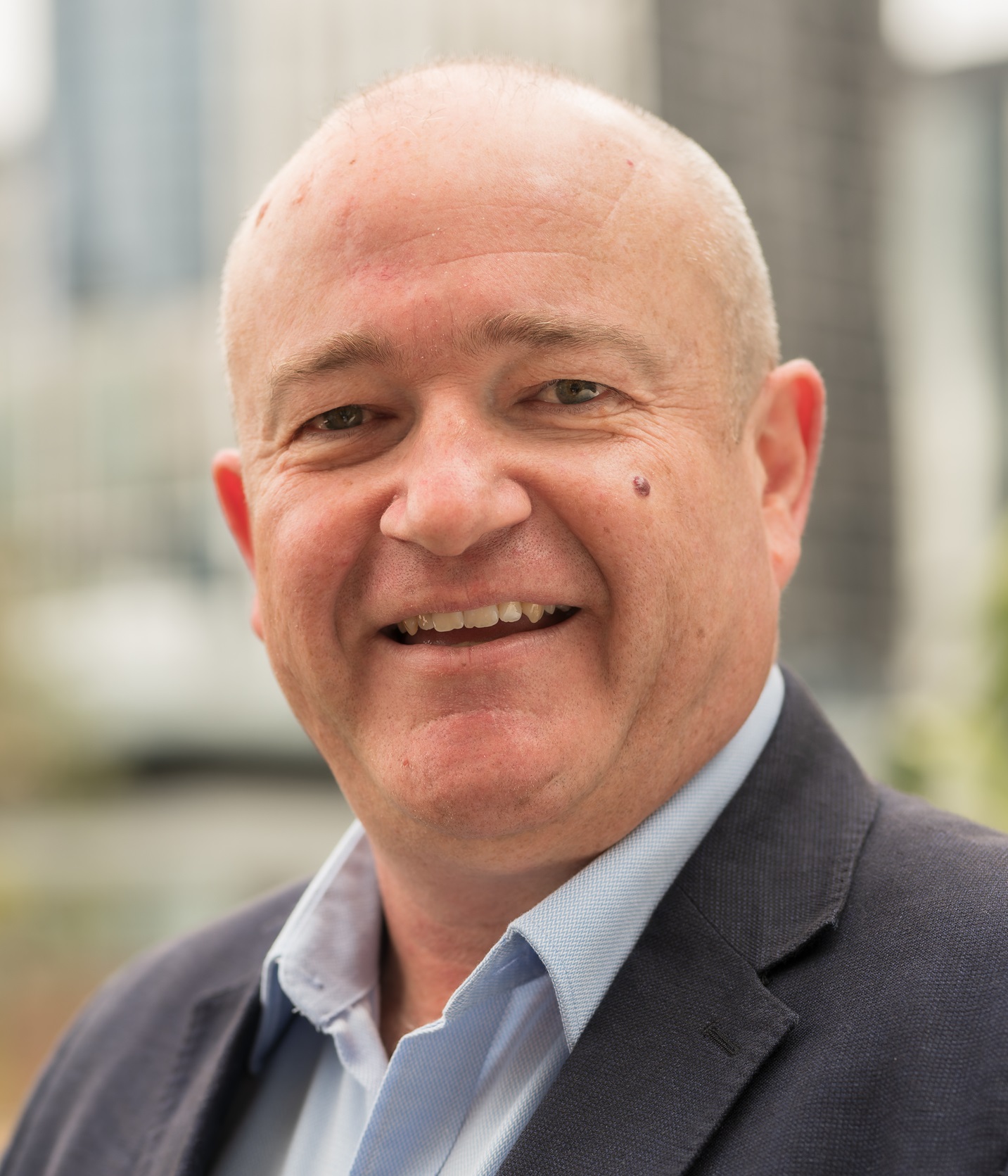
Professor at Univ. Grenoble Alpes (France), Julien Pernot teaches in the Department of Electronics, Electrical Engineering, Control and Systems and carries out research at Institut Néel. Julien obtained his PhD from the University of Montpellier (France) in 2001, where he worked on the electrical transport properties of silicon carbide until 2002. In 2003, he joined the University of Nijmegen (Netherlands) as a postdoc to study defects in wide bandgap semiconductors. At the end of 2003, he was appointed associate professor at Grenoble Alpes University and the Institut NEEL/CNRS. His current research focuses on the electrical transport properties of wide-bandgap semiconductors such as GaN and ZnO, and ultra-wide-bandgap semiconductors such as diamond, AlGaN and AlN for energy conversion and light emission applications. His main scientific contribution concerns innovative devices and electrical measurements carried out on substrate, thin films, microwires or nanowires. At university, he teaches semiconductor physics and electronics. He became a Junior Member in 2012 and a Senior Member in 2024 of the Institut Universitaire de France. He was promoted to Professor in 2016 and awarded the Blondel Medal in 2019. He is co-author of more than 100 articles and a tenth of patents. He is currently deputy director of Institut Néel in charge of innovation and partnership.

Keynote Talk

Prof. Brant Gibson (RMIT University, Australia)

"The future of quantum sensing with diamond"
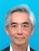
Professor Gibson was awarded his PhD from La Trobe University in 2004. From 2005-09, he was a Photonics Development Engineer at Quantum Communications Victoria (QCV) where he and colleagues designed and developed Australia’s first commercial quantum security product (QCV SPS 1.01). In 2011 he was awarded an Australian Research Council (ARC) Future Fellowship on Hybrid Diamond Materials for Next Generation Sensing, Biodiagnostic and Quantum Devices. Prof. Gibson is currently in the role of Deputy Dean, Research and Innovation, School of Science at RMIT University. He has wide-ranging research interests in the areas of diamond, fluorescent nanoprobes, wide band gap materials, single photon sources, quantum sensors, hybrid nanomaterial integration, fiber optics, photonics, biophotonics, optical, confocal, atomic force microscopy and he has published more than 125 refereed journal publications.
Prof. Hiroshi Kawarada (Waseda University, Japan)

"Diamond MOSFETs for Industrial Applications"
Professor Hiroshi Kawarada received Doctor of Engineering from Waseda University (1985) and joined Osaka University as Assistant Professor (1986) where he started diamond research. Later, he worked in Waseda University as Associate Professor (1990) and Professor (1995-), where he developed C-H diamond FET in 1994. As Visiting Researcher he stayed in Fraunhofer Institute (IAF) by Fellowship of Alexander von Humboldt Foundation (1995-1996). As an organizer he served for European Conference on Diamond and Related Materials (1998-2008). In Japan, he also served for Japan Applied Physics Society as Board Member, New Diamond Forum as Chairman (2009-2014) and Science Council of Japan as Member. His research field is nanoelectronics, bioelectronics and power electronics using diamond, where he has 370 articles with 11,000 citations (Scopus).
Dr. Matthias Schreck (Augsburg University, Germany)

"Presence and future of heteroepitaxial diamond: How to meet the crucial challenges"

Matthias Schreck is research group leader at the Institute of Physics of the University of Augsburg (D). After his diploma degree in Physics obtained from the University of Stuttgart (1987) and a PhD work in Physical Chemistry at the University of Tübingen (1990), both dealing with organic films, he joined University of Augsburg in 1991. There he started CVD diamond activities. His research interests comprised epitaxial growth and structural analysis of oxide, metal, diamond and graphene films. Strong efforts were focused on the mechanisms of heteroepitaxial diamond nucleation on iridium, the scaling of all the relevant synthesis processes to wafer size and the exploration of potential applications such as particle detectors or neutron monochromators. His group developed the multilayer structure Dia/Ir/YSZ/Si and demonstrated in 2017 the first single crystal diamond wafer with a maximum diameter of 92 mm (155 ct). This wafer still represents the state of the art. Together with two colleagues, he founded in 2015 the startup company Augsburg Diamond Technology GmbH (AuDiaTec) – meanwhile sold to Diamond Foundry (USA). Schreck coauthored more than 170 publications and 5 book chapters. After three decades of research focused on “How to realize diamond wafers?”, the major scientific goal for the rest of his career is “What is the highest diamond quality that heteroepitaxy can deliver?”.

Invited Talk

Dr. Khaled Driche (DIAMFAB, France)

"Harnessing Carbon for Power Management: Revolutionizing Device Innovation with Diamond Technology"

Dr. Zhihong Feng (Hebei Semiconductor Research lnstitute, China)

"H-Diamond FETs with High Quality Channel Layer Grown and Fabricated on (001) Single Crystal Diamond Substrate"

Prof. Masazumi Fujiwara (Okayama University, Japan)

"Nanodiamond quantum thermometry for biological applications"

Prof. Jose A. Garrido (ICN2 & ICREA, Spain)

"Graphene thin film technology for neural interfaces"

Prof. Jan Isberg (Uppsala University, Sweden)

"Graphene - on - Diamond Devices"

Dr. Junichi H. Kaneko (Hokkaido University / OOKUMA DIAMOND DEVICE, Japan)

"Beyond the Accident at Fukushima Daiichi Nuclear Power Plant, Toward Social Implementation of Diamond Semiconductors"

Dr. Seongwoo Kim  (Orbray Co., Ltd., Japan)

"World First Free-Standing (111) Heteroepitaxial Diamond without Twin Crystals Grown on Sapphire Substrate"

Dr. Meiyong Liao  (National Institute for Materials Science, Japan)

"Diamond CMOS technology"

Prof. Okhyun Nam  (Tech University of Korea, Republic of Korea)

"Recent Advances in Diamond Power Devices grown on Heteroepitaxial Diamond"

Prof. Mark Newton (University of Warwick, UK)

"Vacancy, nitrogen-vacancy and vacancy cluster production by low energy electron irradiation and annealing in intrinsic and nitrogen doped diamond"

Dr. Shannon Nicley (Michigan State University, USA)

"Quantum Materials Engineering in Diamond: Recent progress on Nickel Vacancies and Other Color Centers"

Dr. Alexandre Tallaire (Institut de Recherche de Chimie Paris, Chimie ParisTech, PSL University, CNRS, France)

"Growth of “quantum-grade” single crystal diamond films and their integration into hybrid structures"

Dr. Volker Weihnacht (Fraunhofer Institute for Material and Beam Technology IWS, Germany)

"New horizons for tetrahedral amorphous carbon films"

Dr. Taro Yoshikawa (Daicel Corporation / Kanazawa University, Japan)

"Visible light-induced photo-emitting diamond electrode for green chemistry applications"

SPECIAL SESSION - R&D in Start-Ups-

Diamfab, France
Diatope, Germany
ExtenD, Japan
Great Lakes Crystal Technologies, USA
HIQUTE Diamond, France
OOKUMA DIAMOND DEVICE, Japan
Power diamond systems, Japan